4xxx Series ICs
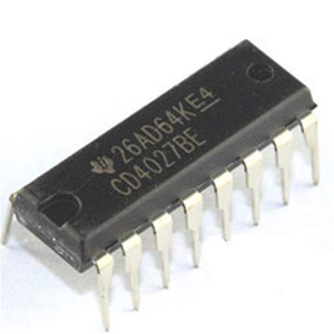
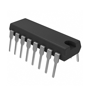
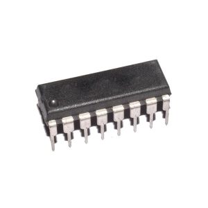
4027 Dual JK Flip Flop with Set and Clear
Product Details
- Fully static operation
- 5 V, 10 V, and 15 V parametric ratings
- Standardized symmetrical output characteristics
- Specified from -40 °C to +85 °C
- Complies with JEDEC standard JESD 13-B
₹29.00 (ex. GST)
The CD4027 is a CMOS based high-speed, high voltage Dual JK Flip-Flop IC. The Flip-flop could operate at a speed of 16MHz at high voltages up to 15V with a low noise margin of ~ 2.5V.
Features
- Dual JK Flip Flop Package IC
- Operating Speed: 16MHz
- Operating Voltage: 5V, 10V, 15V
- Maximum Operating Voltage: 20V
- Input Rise/Fall time at 5V: 45us
- Minimum High-Level Input Voltage: 2 V
- Maximum Low-Level Input Voltage: 0.8 V
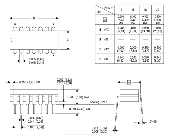
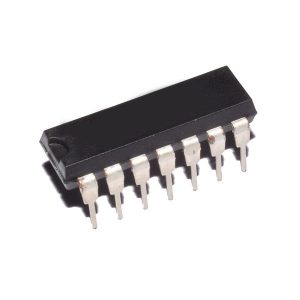
- Available in 14-pin PDIP, GDIP, PDSO packages
- CD4027BMS is a single monolithic chip integrated circuit.
- It contains two identical complementary-symmetry J-K master-slave flip-flops.
- Inputs of each flip-flop: – J, K, Set, Reset, and Clock input signals.
- The output of each flip-flop: – Buffered Q and Q signals.
- This input-output arrangement provides for compatible operation with the CD4013B dual D type flip-flop.
- The CD4027BMS performs: – control, register, and toggle functions.
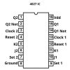
Pin Configuration
| Pin Number | Pin Name | Description |
| 16 | Vcc | Powers the IC typically with 5V |
| 8 | Ground | Connected to the ground of the system |
| For JK Flip Flop – 1 and JK Flip Flop – 2 | ||
| 3,13 | Clock-1/ Clock-2 | These pins must be provided with clock pulse for the flip flop |
| 2,7 | Reset-1 / Reset-2 | Flip flop preset-high will set Q=1 and not Q=0 |
| 4, 12 | Clear-1/Clear-2 | Flip flop cleat-high will set Q=0 and not Q=1 |
| 5, 11 | K-1/ K-2 | Input pin of the Flip Flop |
| 6, 10 | J-1 / J-2 | Another Input pin of the Flip Flop |
| 2,14 | Q-1(bar) / Q-2 (bar) | The inverted output pin of Flip Flop |
| 1,15 | Q-1 / Q-2 | Output Pin of the Flip Flop |
Applications
- Shift Registers
- Memory/Control Registers
- EEPROM circuits
- Latching devices



There are no reviews yet.