
4xxx Series ICs
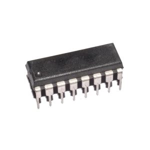
CD4011 Quad 2-Input NAND Gate IC
Features:
- Dual Input NAND Gate – Quad Package.
- Typical Operating Voltage: 5V.
- High-Level Output Current:- 1.5 mA.
- Low-Level Output Current: 1.5mA.
- Propagation Delay Time:60 ns.
₹19.00 (ex. GST)
CD4011 belongs to CD40xx CMOS IC series. This CD4011 IC contains four 2-input independent NAND gates. These gates perform the Boolean function Y = A × B or Y = A + B in positive (+ive) logic. NAND gates in this IC can be reconfigured to make them NOT gate to give inverted output. So we can make SN54LS00 a four NOT gate IC if needed. High-speed NAND operation is possible with this IC because of less transition time and can be used for high-frequency systems.
Features:
- Dual Input NAND Gate – Quad Package.
- Typical Operating Voltage: 5V.
- High-Level Output Current:- 1.5 mA.
- Low-Level Output Current: 1.5mA.
- Propagation Delay Time:60 ns.
- Operating Temperature Range:- 55 C to + 125 C.
- Available in 14-pin PDIP, GDIP, PDSO packages.
Applications:
- AV Receivers.
- Portable Audio Docks.
- Blu-Ray Players.
- Home Theater.
- MP3 Players or Recorders.
- Personal Digital Assistants (PDAs).
Pin Description of CD4011:
| Pin Number | Pin Name | Description |
| 1,2,5,6,8,9,12,13 | NAND Gate Input pins | First Input pin for the NAND gate |
| 3,4,10,11 | NAND Gate Output pins | Output pin for the NAND gate |
| 7 | Ground | Connect to the ground of the circuit. |
| 14 | Vcc (Vdd) | Used to power the IC. Typically +5V is used |

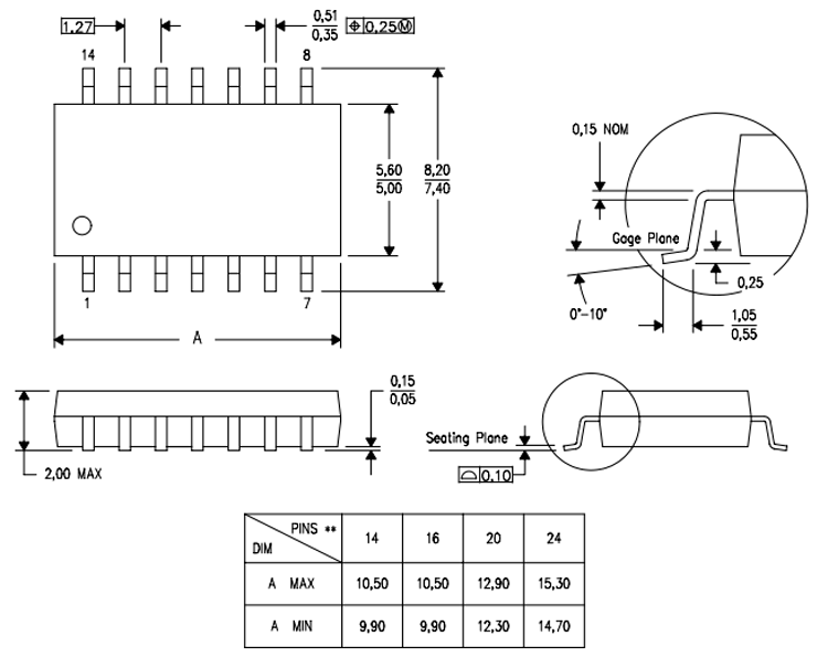
2D LAYOUT/DIMENSION:
Based on 0 reviews
Be the first to review “CD4011 Quad 2-Input NAND Gate IC”
Related products
-
-
Connectors, Wires and Cables, USB Connectors
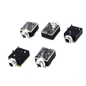
3.5mm Panel Mount Female Audio Jack
Product Details
- Product: Audio jack stereo connector
- Connector type: Female
- Size: 3.5mm
- Material: plastic with strain relief
- Color: black
- Mounting type: panel mount
- Package contains: 1 x 3.5mm Panel Mount Female Audio Jack
SKU: 164
There are no reviews yet.